


Boundary-scan (also called “JTAG Test” after the Joint Test Action Group which developed the technique in the late 1980s) provides a means to test interconnects between integrated circuits on a circuit board “virtually” without using physical test probes.
Despite its promise to reduce testing cost, the added cost of designing boundary-scan circuitry into semiconductor devices has hindered its widespread adoption for a number of years.
However, the increasing density of boards and fine pitch components such as BGAs has significantly diminished the physical accessibility required for in-circuit test. As a result, boundary-scan is growing in popularity as it counteracts the loss of electrical access, increasing fault coverage on the small and very dense boards that are a feature of handheld products such as phone handsets and portable entertainment electronics.
While there are some boundary-scan circuit designs that can effectively eliminate the requirement for in-circuit test, the vast majority of boards still require in-circuit testing, with boundary-scan acting as a vital tool to increase overall fault coverage of the board. In one case, boundary-scan resulted in a 30% increase of fault coverage.
The major advantage of boundary-scan is that no knowledge of actual device function is required to perform thorough interconnect testing. Boundary-scan eliminates the cost and time required to develop and debug traditional digital vector test routines such as those required for ‘backdrive’ in-circuit test.
Boundary Scan Theory of Operation
The IEEE 1149.1 standard specifies the method, hardware and software parameters required to test interconnects among scan devices mounted on a printed circuit board (often called Boundary In-Circuit Test).
To comply with the IEEE 1149.1 standard a boundary-scan chip requires boundary-scan cells at each pin of the device. Each cell is basically a multiplexer and latch. The boundary-scan cell is shown as a small box at each pin in the diagram at right.
In ‘boundary-scan mode’ the latches at each pin are connected serially in a “scan path” (also called a “scan chain”) such that a data pattern is shifted into the latch at each pin via the “TDI” (Test Data In) pin.
Captured test data is serially shifted out via the “TDO” (Test Data Out) pin where it is read by the tester and compared to the expected results.
The Test Access Port (TAP) controller provides the necessary logic to switch the device into and out of ‘boundary-scan mode’ and control the overall test sequence.
Three control lines (TMS, TCK, TRST) perform these required functions in boundary test mode
The second half of the boundary-scan equation is the software required to:
Most available boundary-scan tools provide rigorous algorithms to stimulate and detect faults and to isolate faults to specific nets, devices, and pin numbers. The majority of these tools employ the Boundary-scan Description Language (BSDL). BDSL specifications were added to the IEEE 1149.1 standard in 1994.
A variety of boundary-scan tool vendors supply boundary-scan stimulus/measurement software and hardware adaptor tools, which can be added to any CheckSum Analyst system.
Low Cost Partnership Case History: Boundary Scan and Analyst In Circuit Test
A major contract manufacturer sought a way to implement boundary scan for a new board it was building but saw no point in purchasing an expensive traditional in-circuit tester such as those from Teradyne or Agilent just to obtain boundary scan capability. CheckSum provided a low-cost boundary scan test solution for under $70,000, including the cost of the Analyst ems in-circuit tester and boundary scan tools from a popular boundary scan technology supplier.
The circuit board was approximately 5 inches by 11 inches (12.7 x 17.8 cm) with 1,200 electrical nets, of which only 810 could be physically probed and tested using conventional ICT techniques. As is typical with modern devices, speed and functional complexity precluded using traditional vector-based ‘backdrive’ testing.
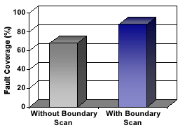
By adding boundary scan test, the contract manufacturer upped the total to 1,050 tested nets, boosting fault coverage from 68% to 88%–a 30% increase. In addition, the board included 40 ICs, the largest being an 860-pin ASIC. All of them were testable with boundary scan.
One-time charges were approximately $55,000 for the Analyst tester and $15,000 for the third-party hardware and software. Recurring costs of test for similar boards requiring boundary scan test would be only about $12,000 for the bed-of-nails test fixture in-circuit program and boundary scan test.
Boundary Scan Can Reduce Board Test Costs
A major goal of boundary scan test is to reduce test cost while maximizing test coverage. This contract manufacturer understood that implementing boundary scan on a traditional ICT contradicted the cost and simplicity goal of boundary scan. The CheckSum Analyst low cost in-circuit tester, on the other hand, is consistent with those objectives.


