


Boundary-scan (also called “JTAG Test” after the Joint Test Action Group which developed the technique in the late 1980s) provides a means to test interconnects between integrated circuits on a circuit board “virtually” without using physical test probes.
Despite its promise to reduce testing cost, the added cost of designing boundary-scan circuitry into semiconductor devices has hindered its widespread adoption for a number of years.
However, the increasing density of boards and fine pitch components such as BGAs has significantly diminished the physical accessibility required for in-circuit test. As a result, boundary-scan is growing in popularity as it counteracts the loss of electrical access, increasing fault coverage on the small and very dense boards that are a feature of handheld products such as phone handsets and portable entertainment electronics.
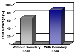
While there are some boundary-scan circuit designs that can effectively eliminate the requirement for in-circuit test, the vast majority of boards still require in-circuit testing, with boundary-scan acting as a vital tool to increase overall fault coverage of the board. In one case, boundary-scan resulted in a 30% increase of fault coverage.
The major advantage of boundary-scan is that no knowledge of actual device function is required to perform thorough interconnect testing. Boundary-scan eliminates the cost and time required to develop and debug traditional digital vector test routines such as those required for ‘backdrive’ in-circuit test.
Boundary Scan Theory of Operation
The IEEE 1149.1 standard specifies the method, hardware and software parameters required to test interconnects among scan devices mounted on a printed circuit board (often called Boundary In-Circuit Test).
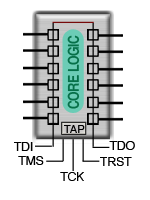
To comply with the IEEE 1149.1 standard a boundary-scan chip requires boundary-scan cells at each pin of the device. Each cell is basically a multiplexer and latch. The boundary-scan cell is shown as a small box at each pin in the diagram at right.
In ‘boundary-scan mode’ the latches at each pin are connected serially in a “scan path” (also called a “scan chain”) such that a data pattern is shifted into the latch at each pin via the “TDI” (Test Data In) pin.
Captured test data is serially shifted out via the “TDO” (Test Data Out) pin where it is read by the tester and compared to the expected results.
The Test Access Port (TAP) controller provides the necessary logic to switch the device into and out of ‘boundary-scan mode’ and control the overall test sequence.
Three control lines (TMS, TCK, TRST) perform these required functions in boundary test mode
The second half of the boundary-scan equation is the software required to:
Most available boundary-scan tools provide rigorous algorithms to stimulate and detect faults and to isolate faults to specific nets, devices, and pin numbers. The majority of these tools employ the Boundary-scan Description Language (BSDL). BDSL specifications were added to the IEEE 1149.1 standard in 1994.
A variety of boundary-scan tool vendors supply boundary-scan stimulus/measurement software and hardware adaptor tools, which can be added to any CheckSum Analyst system.
Low Cost Partnership Case History: Boundary Scan and Analyst In Circuit Test
A major contract manufacturer sought a way to implement boundary scan for a new board it was building but saw no point in purchasing an expensive traditional in-circuit tester such as those from Teradyne or Agilent just to obtain boundary scan capability. CheckSum provided a low-cost boundary scan test solution for under $70,000, including the cost of the Analyst ems in-circuit tester and boundary scan tools from a popular boundary scan technology supplier.
The circuit board was approximately 5 inches by 11 inches (12.7 x 17.8 cm) with 1,200 electrical nets, of which only 810 could be physically probed and tested using conventional ICT techniques. As is typical with modern devices, speed and functional complexity precluded using traditional vector-based ‘backdrive’ testing.
By adding boundary scan test, the contract manufacturer upped the total to 1,050 tested nets, boosting fault coverage from 68% to 88%–a 30% increase. In addition, the board included 40 ICs, the largest being an 860-pin ASIC. All of them were testable with boundary scan.
One-time charges were approximately $55,000 for the Analyst tester and $15,000 for the third-party hardware and software. Recurring costs of test for similar boards requiring boundary scan test would be only about $12,000 for the bed-of-nails test fixture in-circuit program and boundary scan test.
Boundary Scan Can Reduce Board Test Costs
A major goal of boundary scan test is to reduce test cost while maximizing test coverage. This contract manufacturer understood that implementing boundary scan on a traditional ICT contradicted the cost and simplicity goal of boundary scan. The CheckSum Analyst low cost in-circuit tester, on the other hand, is consistent with those objectives.
Roll your mouse over the topics in the column at the right for a quick review of testing techniques for ICs on boards, their advantages and disadvantages.
Testing ICs on Circuit Boards (In-Circuit Test): a brief tutorial
Delivers High Fault Coverage for the Least Cost
Opens around ICs–whether pins or internal problems–are the most prevalent fault class on virtually every SMT manufacturing floor. If you’re in circuit testing boards but skipping vectorless test you’re either wasting money, adversely impacting board quality–or both.
Power-off vectorless test is superior to classical digital vector test (aka „backdrive” test) in just about every IC testing situation. And TestJet is the most widely used vectorless test technology in the world.
But if you’re still using traditional 'big iron’ in circuit testers like Agilent and Teradyne to program and perform vectorless test you’re spending too much. Why?
Why CheckSum Analyst systems are your best tool for TestJet vectorless test
CheckSum Analyst systems use exactly the same TestJet Technology originally introduced by Hewlett-Packard (now Agilent) in 1994 and now used on thousands of in circuit testers worldwide. TestJet Technology reliably identifies opens around (and inside) almost any IC package with a lead frame or metallic pins or leads to which the TestJet probe can capacitively couple–an enormous variety of device types.
| Device Type / Package |
Use TestJet Technology? |
|
| Devices with an internal lead frame (most digital and hybrid devices) | Yes | |
| Devices with an internal ground plane (usually ceramic packages) | No | |
| Most Ball Grid Arrays (BGAs) (except ceramic and stadium packages) | Yes | |
| Some Ball Grid Arrays (CBGAs) (ceramic and stadium packages only | No | |
| Connectors and sockets | Yes | |
| Devices with grounded heat sink | No | |
| Flip chip devices or chip-on-board | No | |
| DIP switches | Yes | |
| Pushbuttons | No |
TestJet Technology is the ideal match to Analyst’s low cost and ease of application. Unburdened by expensive digital vector hardware and software, Analyst systems equipped with TestJet Technology create an unbeatable combination of low applications (fixture and test program) cost, fast throughput and high fault coverage.
The inside story: TestJet Technology
TestJet Technology examines the connectivity from each pin on a device to the circuit board. It does not require that power be applied to the device under test.
The TestJet hardware measures the capacitance from a pin of a device to the TestJet probe. The measured value is compared against preset limits by the Analyst system–just like any other in circuit test. If the capacitance falls below the lower tolerance an open pin exists. This measurement is repeated for each pin on the device except power and ground pins. Pins that are tied together are tested as one pin.
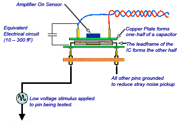
A specific test step is accomplished by connecting a low voltage AC stimulus source to the pin being tested, the Sense to the TestJet probe, and then to guard out (ground) all other pins on the device. The signal is amplified and filtered right at the TestJet probe to improve signal quality. Each TestJet probe is connected to a port on a system TestJet board that is mounted in the test system chassis. Depending on the specific test system configuration, up to 384, or more, TestJet probes can be connected to the test system.
Features
Application
Programming CPLDs (Complex Programmable Logic Devices) such as serial flash memories and microcontrollers after these parts have been mounted on the printed circuit board. Since the contents of Phase Change Memory (also known as PCM, PCME, PRAM, PCRAM, and C-RAM) can be lost because of the high temperatures needed to solder the device to a board, on-board programming is required.
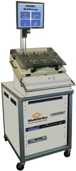
The MultiWriter pps™ on-board gang programming system uses proven, patented simultaneous programming technology to program up to 384 chips simultaneously, up to 16 different types or families — typically in seconds instead of the minutes required by conventional programmers.
Compared to other part programming solutions, MultiWriter pps delivers significant speed and cost advantages over conventional in-circuit tester-based programmers when more than four parts already mounted on circuit boards must be programmed in a single pass, making it especially effective for multi-board panels.
MultiWriter pps is optimized for applications requiring programming of at least 4 parts per board or multi-board panel. MultiWriter can simultaneously program parts on multi-board panels with 10, 20 or more boards per panel.
Advantages of On-board Part Programming with the MultiWriter pps
Product Details
The MultiWriter pps On-board Gang Programming System includes:
Purchase or Pay-Per-Use
Is Pay-Per-Use the right solution for your programmed parts?
† MultiWriter Technology is protected under U.S. Patent No. 7,802,021.

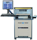
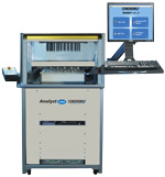
Analyst In Circuit Test Systems
High-coverage In Circuit Test (ICT)
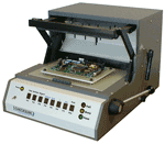
The CheckSum Analyst ems is designed to test all types of circuit assemblies. The system combines manufacturing process testing with TestJet Technology to test a single assembly or a panel of multiple assemblies.

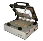
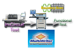
MultiWriter Part Programming
In Circuit On-Board Part Programming
On-Board, Production Part Programming for up to 384 devices simultaneously means high-throughput at low cost.
Test fixtures

Reliability at low cost
Reliable low-cost test fixtures from CheckSum.
Turnkey support
Custom fixtures & test programs
Only CheckSum offers complete ready-to-run turnkey applications packages so your boards are in production fast.
New Circuit Board Technology Requires New Strategic Thinking
Circuit board technology evolves rapidly: more highly integrated devices, increasing package pin counts, denser placement of smaller components and thinner circuit traces. For boards ranging from simple to complex, the test and inspection process remains as critical as ever. Bad parts still find their way onto boards. Assembly and soldering defects still occur. In-circuit test (ICT) is still the most cost effective means to identify component faults and manufacturing process defects. And as long as there are circuit boards, ICT will continue to be the key to effective manufacturing process test.
But evolving technology requires a complete rethinking of in-circuit test strategy—and about the in-circuit tester itself.
Traditional ICT capabilities are increasingly expensive—and unnecessary
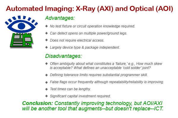
The Fault Spectrum Shift has basically negated the cost effectiveness of traditional ICT testers such as the Agilent 3070-series and Teradyne TestStation. Capabilities found on these testers such as high-accuracy analog and digital vector test are increasingly superfluous because they are designed to test for faults that rarely—if ever—occur on today’s boards. In fact, traditional digital vector test is ineffective on today’s complex, highly integrated devices. And newer assembly defect classes such as cold solder joints and skewed components are simply invisible to in-circuit testers and must be diagnosed by other means such as automated imaging (AOI, AXI).
Evolving technologies aren’t the only reason you should reexamine your ICT strategy and equipment. Today’s smaller test departments and constrained budgets demand lower ICT costs. In a fixed budget environment every dollar you spend unnecessarily on ICT means a dollar that you can’t invest in new inspection technologies like AOI and AXI.
The Low Cost ICT strategy
Seeking a lower-cost ICT strategy demands that you examine not only the purchase price of the tester, but also ongoing operating and applications cost, such as fixturing, programming, and support. Keep in mind that no matter how low the purchase price, “big iron” ICT still has high overhead costs from complex test fixtures and lengthy test programming processes—even when built-in capabilities like vector testing are not even used.
The good news about new board and parts technologies and the resulting Fault Spectrum Shift is that much lower cost ICT systems will do the job as effectively as old, expensive ones. That’s where the CheckSum Analyst Low Cost In-Circuit Testers come in. Check them out and see how CheckSum can reduce testing cost and help increase manufacturing margins.
Analyst ems 12KN
High-coverage in circuit test
Capable. Flexible. Straightforward. The CheckSum Analyst ems combines comprehensive manufacturing process testing with TestJet Technology for low cost in circuit test of today’s complex boards.
Analyst ems+ft 12KN
In circuit and functional test
The Analyst ems+ft combines all the in circuit capability of the Analyst ems with versatile power-on functional test, including relays capable of switching up to 250VAC (rms), full DMM, function generator and counter-timer for simple test routines to full functional test sequences.
Analyst ems TR-3-Console
Vacuum-based in circuit test
The Analyst ems TR-3-Console is an integrated rack/console system with vacuum-based fixturing.
Analyst ils
In-line in circuit test
The Analyst ils integrates the in circuit testing capability of the Analyst platform into an automated in-line board handling system–at a price less than many manually operated in circuit testers.

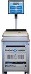
Analyst ems
In circuit test
The Analyst ems can be integrated with desktop pneumatic or mechanical type fixture systems. These low-cost test and fixture systems require a small space.
Founded in 1987, CheckSum has been delivering reliable, cost-effective, and flexible in-circuit test and on-board, in-system programming solutions to OEMs and contract manufacturers (CM). With an installed base of over 3,000 test systems at more than 200 manufacturing sites in over 40 countries, CheckSum’s customers range from automotive electronics manufacturers to global EMS / CM providers.
CheckSum’s practical production test and on-board, in circuit, part programming solutions help its customers reduce total test and manufacturing costs and increase profit margins.
Read these customer case histories and newsletters to see how CheckSum delivers solutions that meet the demanding technical requirements while reducing total cost:
![]()
Tier 1 Contract Manufacturer Cuts Programming Cost by 66%
On-Board Part Programming with Pay-Per-Use
How One Manufacturer Slashed
In-Circuit Test Cost by 60%
CheckSum’s Analyst Works
Side-By-Side with ’Big Iron’ In Circuit
Testers at a Fraction of the Cost
An OEM finds the Analyst is the
Ideal Platform for Boundary Scan
Test and High Throughput In Circuit
Part Progamming
Contract Manufacturer (CM) Implements
Boundary Scan Test on a New Board with
CheckSum’s Analyst In Circuit Test System
Fault Coverage Improves 30%
Managing Your Tester Portfolio and
Achieving a Low Cost Board Test Strategy
Many test engineers seek to „standardize” on a single brand or model in circuit tester. Intuitively, this makes sense: only one vendor to deal with, common fixturing, a single programming environment, simplified support. In order to deal with any board of any complexity, it seems to also make sense to standardize on traditional high-end in circuit tester that has all the reserve horsepower–high accuracy analog, sophisticated digital backdrive, functional test facilities, etc.–that the test engineer might ever need.
ICT Platform „Standardization” Means Higher Cost of Test
But traditional „big iron” ICT always drives up overall test cost–even when it’s the „standard” that’s supposed to reduce overall test cost. The theoretical savings of a “standard” rarely offsets the high fixturing, programming and support costs that traditional ICTs entail. A high capability tester is absolutely right for a high complexity board. But putting a simpler board on a „big iron” ICT is analogous to planting a rosebush with a backhoe: The job gets done, but it’s a lot more complicated and expensive compared to putting the less complex board on a less complex tester that has lower application and support costs.
Tester Portfolio Management is Straightforward
Just as a portfolio manager maximizes investor return by using a variety of investment vehicles, the „tester portfolio manager” will distribute test jobs between the „big iron” ICT and the Low Cost ICT based on criteria such as board complexity and production volume. This way, lower cost testers, fixtures and programs test boards that don’t require expensive capabilities like digital backdrive. Complex boards, such as those with specialized low-voltage chips are tested on machines with the required tester resources.
Tester Portfolio Management Saves Money
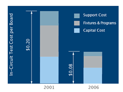
Tester Portfolio Management reduces total test cost by avoiding unnecessary tester overhead for test jobs that don’t require expensive „big iron” test capabilities–especially digital vector test (aka 'backdrive’). Because Low Cost ICT does away with the inherent complexity of digital test not only is the tester itself simpler and less expensive, but fixtures and programs, too. One user who implemented the same board on both types of testers experienced a greater than 75% cost savings in applications cost (fixture + test program) on the Low Cost ICT. Check out a similar case for yourself.
Consider Test Cost Up Front. Not After It’s Too Late.
When implementing new test jobs seek the lowest cost test solution by evaluating the total test cost ahead of time– even if it means investing in a „non-standard” Low Cost ICT . Today, „big iron” and Low Cost ICT coexist on an increasing number of test floors delivering much lower total testing cost than a single high-end „standard.” Even though building a tester portfolio instead of a single standard seems counterintuitive. That’s what a major automotive electronics manufacturer thought until they reduced test cost by more than 60% without any increased „escapes” to functional test.
Improve manufacturing margins by reducing test cost
Test is necessary but wasteful because it adds no value to the product. In today’s world of tight manufacturing margins circuit board test is an ideal cost reduction target. Yet, many OEMs and contract manufacturers (CMs) continue to generate unnecessary cost—and reduce their margins—by continuing to put every test job on their expensive ‘big iron’ in circuit testers with their high fixturing, programming and support costs.
CheckSum estimates that by sticking with traditional ‘big iron’ ICTs instead of investing in Low Cost ICT, OEMs and CMs unnecessarily spend more than $250 million per year in additional test cost. In a world where every margin dollar makes a difference, reducing that unnecessary cost is an ideal way to improve the manufacturing bottom line.
The example at right illustrates how a contract manufacturer with 5% gross margins can add 40 basis points to its gross margin—an 8% improvement—by reducing circuit board test costs by just 10%. One Tier 1 manufacturer found that it could reduce in circuit test cost by 60%. Even if ICT cost represents just half of total board test cost, that’s a 30% cost reduction.
CMs who have recognized and seized this cost reduction opportunity are enjoying both increased operating margins and competitive advantage. OEMs who recognize that test costs can be reduced are well positioned to negotiate lower overall prices from their CM.
3 steps to reduce board test cost
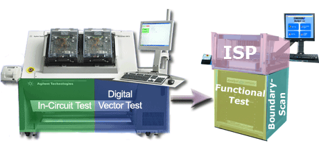
Myślenie poza jedną platformą w strategii testu.
Duże stałe testery obwodów sprzedawane są od lat jako platforma „robiąca wszystko”: analogowe w obwodzie; cyfrowy test wektorowy (backdrive), test wektorowy, programowanie ISP, skanowanie granic, test funkcjonalny oparty na oprzyrządowaniu itp.
Ujednolicenie wszystkich tych zadań może uprościć i ujednolicić zadanie grupy testowej, bez względu na to, jakie niespodziewane nowe technologie mogą wysłać projektanci produktu. Nie ma dodatkowego wyposażenia uzasadniającego zarządzanie i kupowanie. Personel jest już przeszkolony w zakresie korzystania z systemu. Wielki dostawca testerów stałych mówi: „Po prostu dodaj opcjonalny sprzęt i oprogramowanie, a będziesz gotowy”.
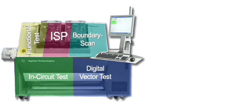
Ale rzeczywistość jest zawsze bardziej skomplikowana.
Strategia testu dwustopniowego
Na początku wydaje się to sprzeczne z intuicją, ale wdrożenie nowych testów na nowej, taniej platformie może drastycznie uprościć ogólne zadanie, przyspieszyć przepustowość i kosztować znacznie mniej niż próba zintegrowania wszystkiego w dużymstałym testerze. W jaki sposób?
New Circuit Board Technology Requires New Strategic Thinking
Circuit board technology evolves rapidly: more highly integrated devices, increasing package pin counts, denser placement of smaller components and thinner circuit traces. For boards ranging from simple to complex, the test and inspection process remains as critical as ever. Bad parts still find their way onto boards. Assembly and soldering defects still occur. In-circuit test (ICT) is still the most cost effective means to identify component faults and manufacturing process defects. And as long as there are circuit boards, ICT will continue to be the key to effective manufacturing process test.
But evolving technology requires a complete rethinking of in-circuit test strategy—and about the in-circuit tester itself.
Traditional ICT capabilities are increasingly expensive—and unnecessary
The Fault Spectrum Shifthas basically negated the cost effectiveness of traditional ICT testers such as the Agilent 3070-series and Teradyne TestStation. Capabilities found on these testers such as high-accuracy analog and digital vector test are increasingly superfluous because they are designed to test for faults that rarely—if ever—occur on today’s boards. In fact, traditional digital vector test is ineffective on today’s complex, highly integrated devices. And newer assembly defect classes such as cold solder joints and skewed components are simply invisible to in-circuit testers and must be diagnosed by other means such as automated imaging (AOI, AXI).
Evolving technologies aren’t the only reason you should reexamine your ICT strategy and equipment. Today’s smaller test departments and constrained budgets demand lower ICT costs. In a fixed budget environment every dollar you spend unnecessarily on ICT means a dollar that you can’t invest in new inspection technologies like AOI and AXI.
The Low Cost ICT strategy
Seeking a lower-cost ICT strategy demands that you examine not only the purchase price of the tester, but also ongoing operating and applications cost, such as fixturing, programming, and support. Keep in mind that no matter how low the purchase price, “big iron” ICT still has high overhead costs from complex test fixtures and lengthy test programming processes—even when built-in capabilities like vector testing are not even used.
The good news about new board and parts technologies and the resulting Fault Spectrum Shift is that much lower cost ICT systems will do the job as effectively as old, expensive ones. That’s where the CheckSum Analyst Low Cost In-Circuit Testers come in. Check them out and see how CheckSum can reduce testing cost and help increase manufacturing margins.
Circuit Boards Have Changed.
So Has The Board Test Fault Spectrum.
Over the past several years printed circuit board assembly yields have increased as component and assembly process defect rates have decreased as shown in the figure on the right. In addition, the distribution of fault types typically found on boards during the manufacturing and assembly process has shifted over the past several years as illustrated in the fault spectrum pie diagrams to the right.
Why Does the Shifted Fault Spectrum Matter? Because the Fault Coverage of Traditional In Circuit Testers Is Declining.
The Shifted Fault Spectrum also means that the faults that traditional ICT is adept at finding occur much less frequently—reducing overall tester effectiveness—but not cost.
As a Result
Test engineers have eliminated almost all of the tests traditional ICT was designed to do well—resulting in simple in circuit programs that leave all that „big iron” ICT capability either under-used or unused. This mismatch between today’s fault spectrum and yesterday’s traditional ICT means high overhead costs for unused tester resources in the form of more complicated fixtures and programs and the higher support costs inherent in complex testers.
New Technologies Will Augment In Circuit Test (ICT)
While ICT remains the most economical means to identify manufacturing and component defects, new technologies such as Automated X-Ray Inspection (AXI) and Automated Optical Inspection (AOI) are being integrated into assembly lines to deal with the new defect classes that ICT can no longer—or simply never could—identify.
What Does the Shifted Fault Spectrum Mean For ICT?
If test engineers continue to use traditional „big iron” ICT for every test job, OEMs and contract manufacturers will keep generating unnecessary test costs. For North America alone, CheckSum estimates that more than $250 million annually is spent unnecessarily on testers, tester support, test programs and fixtures by using „big iron” where Low Cost ICT will do the job. Employing Tester Portfolio Management will reduce total ICT cost while maintaining superior fault coverage–and free up budgets to fund the new AOI and AXI technologies that today’s new board technologies also require.


